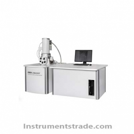
KYKY-EM8100F FEG SEM Thermal Field Emission Scanning Electron Microscope Introduction
Scanning electron microscopy (SEM) is a microscopic morphology observation method between transmission electron microscope and optical microscope. It can directly use the material properties of the sample surface material for microscopic imaging. Features
Schottky Schottky field emission electron gun, high brightness, good monochromaticity, small electron beam spot, long life
Achieve breakthrough in domestic low-pressure mode parameters
Electron beam acceleration tube
High beam stability and small dispersion, suitable for long-term accurate analysis, such as BSE, EDS, EBSD, etc.
Low accelerating voltage non-conducting samples can be directly observed without the need to spray gold
Easy to operate, with a trackball console, you can also use the mouse to complete all EM operations
Equipped with large-stroke sample stage, electron beam exposure, optional freezer, stretching table, nano-operator, compatible with most domestic or imported accessories
Can realize non-standard customization of optics, sample stage, etc. Technical Parameters
Resolution: 1 nm (30KV); 3nm (1KV)
Magnification: 15x~800,000x
Acceleration voltage: 0 ~ 30KV
Electron gun: Schottky Schottky field emission electron gun
Auto adjustment function: focus, brightness/contrast, astigmatism, electron beam pair medium
Vacuum system: High vacuum secondary electron detector, four-segment backscattered electron probe (with the function of protecting the detector probe from collision)
stroke:
X: 0 ~ 150mm
Y: 0 ~ 150mm
Z: 0 ~ 60mm
R: 360°
T: -5° ~ 75° (maximum sample diameter 375mm)
Detectors: SE detector, BSE detector, X-ray spectrometer (optional), EBSD (optional), etc.
Scanning electron microscopy (SEM) is a microscopic morphology observation method between transmission electron microscope and optical microscope. It can directly use the material properties of the sample surface material for microscopic imaging.