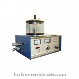
Introduction: The ETD-900C ion sputtering instrument has beautiful appearance and exquisite workmanship. The company has developed and produced a multi-purpose equipment that can sputter gold, silver, copper, platinum and evaporate carbon film for SEM users. This machine has the advantages of small size, convenient operation, simple operation, and good film-forming effect, which can meet the needs of SEM users for sample preparation at any time. It is easy to control the pressure of the vacuum chamber, ionization current and select the required ionization gas by combining the internal automatic control circuit when working to obtain the best coating effect. Equipped with high-position qualitative Feiyue vacuum pump use: 1. Electron beam sensitive samples Mainly include biological samples, plastic samples, etc. The electron beam in S EM has high energy. During the interaction with the sample, it transfers part of the energy to the sample in the form of heat. If the sample is a material sensitive to electron beams, this interaction will destroy part or even the entire sample structure. In this case, a surface coating made of a non-electron beam sensitive material can act as a protective layer to prevent such damage; 2. Non-conductive samples Since the sample does not conduct electricity, its surface has "electron traps". This accumulation of electrons on the surface is called "charging". In order to eliminate the charging effect, a metal conductive layer can be plated on the surface of the sample. The coating acts as a conductive channel to transfer the charged electrons from the surface of the material to eliminate the charging effect. In scanning electron microscopy imaging, sputtering materials increase the signal-to-noise ratio, thereby obtaining better imaging quality. 3. New materials Fabrication of experimental electrodes of non-conductive materials to observe conductive characteristics Technical Parameters: Sputtering gas: Argon, nitrogen and other gases can be added according to the purpose of the experiment. Sputtering target: The standard target is a gold target with a thickness of 50mm*0.1mm. Silver targets, platinum targets, etc. can also be equipped according to actual conditions. The evaporation material is carbon rope. Sputtering current: maximum current 50mA, maximum working current 30mA Sputtering rate: better than 4nm/min Sample bin size: diameter 160mm, height 120mm Sample stage size: The sample stage size can be installed with a sample stage with a diameter of 50mm and a diameter of 70mm, and the height of the sample stage can be adjusted. The sample table can also be customized according to your own requirements Working voltage 220V (110V can be used), 50HZ